|
Home | |
Sitemap | |
Contact | 简体 | 繁体 |
 |
 |
 |
 |
 |

|
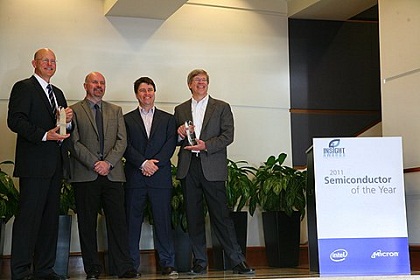
SAN JOSE, Calif.--"As long as the insatiable thirst for memory exists, we will always continue to beat Moore's Law," said Ramin Ghodsi, Micron Technology Inc.'s senior director of NAND development, at an award ceremony naming Intel Corp. and Micron's 20-nm NAND flash the Semiconductor of the Year.
Intel and Micron were selected by UBM TechInsights in its 10th annual Insight Awards for their joint development project to create 20-nm NAND flash technology, thought to represent a big breakthrough in terms of storage for consumer and compute applications.
The high-capacity, multilevel cell (MLC) NAND made on the 20-nm process is already in volume production and is ready to slot straight in to solid-state drives (SSDs),smartphones, tablets, computers, e-book readers and much more besides.
Micron and Intel's20-nm MLC NAND flash, manufactured by their IM Flash Technologies joint venture, was the first to be manufactured at the 20-nm process node and further impressed by replacing the traditional silicon dioxide gate with a high-k dielectric, allowing for reduced cell leakage and low power consumption.
Glen Hawk, vice president of Micron's NAND solutions group, told EE Times that winning the award was "an incredible honor" and capped off what he felt to be one of the industry's best partnerships.
"I'm continuously astounded by what our two companies are able to achieve together," he said, noting that despite the differences in company cultures, the two worked very synergistically together, attaining "fantastic results."
Hawk himself, one of the product's "founding fathers" has been on both sides of the partnership, having moved from Intel to Micron after the first stages of brokering the initial cooperation between the two.
Rob Crooke, vice president and general manager from Intel's NVM solutions group, said that with Micron's tremendous knowledge on high volume memory manufacturing and Intel's expertise on materials, cell and process technology, the two had achieved something of a design dream team.
"We're confident that the technology we've created here scales into the future," he said, noting that the firms were already working on the next steps,
after updating their mutual agreements, to expand into other technologies
.
"We're not quite ready to talk about those technologies because they're still in research, but they will be based around both the future of NAND and some alternative technologies as well," he promised.
"We have a lot to offer in the years to come," added Hawk.
In order to permit for future scaling, and pushing down past the 20-nm process node, Hawk said the high-k dielectric metal gate cell structure had been key, and was the innovation that would allow the firms to continue to scale.
Ghodsi noted that the conventional scaling path adopted by many of the firms' competitors actually amounted to some rather difficult geometries when it came to some of the structures, while Micron's move to a planar cell structure allowed for more structures to be fit into a smaller space.
"As you increase the density of the memory, the number of bits per unit is increasing so much that you also have to deal with energy consumption, power consumption, so there's a lot of innovations in that area as well," he added.
| Corporate Profile │ Quality Commitment │ Contact │ Sitemap │ Join Us |
| Copyright © 2002-2018 True Sources All Rights Reserved. 粤ICP备17159005号-2 |